
Photonics has an unusual shape as an industry. The chip is comparatively solved. Getting light onto it is not.
The bottleneck is not the chip
Silicon photonics was attractive because it promised to reuse the semiconductor industry's manufacturing base. Waveguides, modulators, splitters and detectors can be patterned on silicon wafers with the same lithography that makes transistors, which means volume, yield learning and existing capital.
That part has largely worked. The part that has not scaled the same way is everything that happens after the wafer.
An optical fibre core is a few micrometres across. A silicon waveguide is smaller and shaped differently. Coupling light between them efficiently requires alignment to a fraction of a micrometre, held against temperature change and mechanical stress for the life of the product. Get it wrong by a small amount and you lose a large fraction of the light, which in a communications link is the entire power budget.
Electronics is connected with solder, which is forgiving. Photonics is connected by alignment, which is not.
Three further complications make packaging the dominant cost in many photonic products.
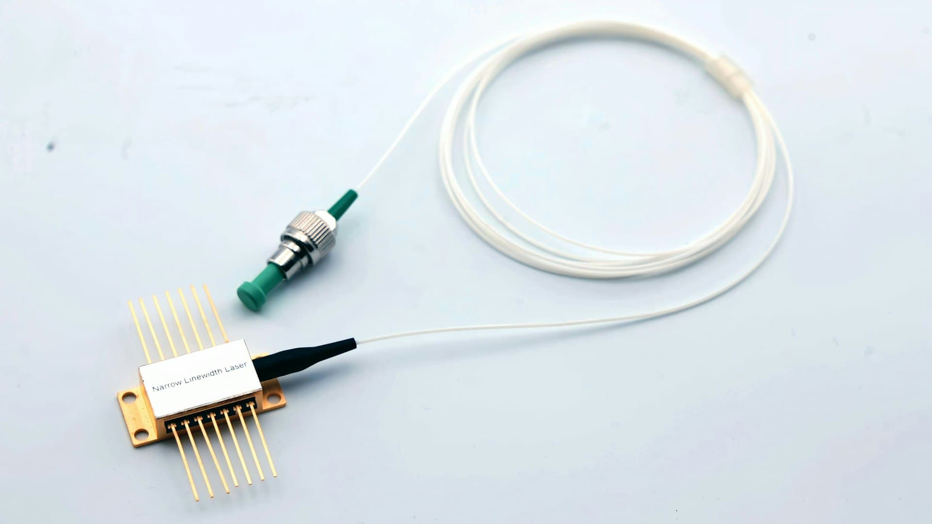
Lasers are usually a separate material. Silicon does not emit light efficiently, so most systems attach a laser made from a compound semiconductor, which means a bonding or assembly step with its own alignment and thermal requirements.
Testing needs optical access. Electrical probing of wafers is highly automated. Optical testing requires getting light in and out, which is slower and less automated, and testing before packaging is difficult precisely because the coupling structures are the thing under test.
The processes are less standardised. Electronic packaging has decades of shared infrastructure. Photonic packaging is more varied between companies and products, which limits the learning that would drive cost down.
This is why photonic packaging engineers and optical assembly technicians are among the harder roles to fill in the industry, and why the skill is worth building deliberately rather than hoping to hire it.
What the direction covers
The scope: optics, lasers, fibre optics, optical communications, photonic integrated circuits and optical sensing.
Four areas.
Optical fundamentals. Propagation, loss, dispersion, polarisation, coupling and the noise sources that set link budgets.
Sources and detectors. Lasers, modulators, photodiodes and the electronics that drive and read them.
Integration. Photonic integrated circuits, waveguide design, and the interface between photonic and electronic layers.
Packaging and test. Alignment, attachment, thermal management and optical measurement.
Why data centres are reaching for light
The interest in co-packaged optics, where optical engines sit on the same package substrate as the switch or accelerator chip, is not aesthetic. It comes from two limits arriving at once.
Electrical signalling loses reach as it speeds up. Pushing higher data rates down a copper trace costs signal integrity, and the distance a link can cover at a given rate keeps shrinking. Eventually the copper cannot reach from the chip to the faceplate, which is where a pluggable optical module sits today.
The interface power is no longer negligible. Driving high speed electrical links and running the retiming and equalisation they need consumes a share of system power that has grown from an afterthought into a budget line, particularly in machine learning clusters where the interconnect is a large fraction of the machine.
Moving the optical conversion from the faceplate to the package shortens the electrical path dramatically, which recovers both reach and power. That is the argument, and it is a sound one.
The counter-argument deserves equal space, because it is why adoption has been slower than the roadmaps suggested. A pluggable module can be replaced in minutes by a technician. An optical engine bonded into a package cannot. If the laser fails, the failure is now inside a very expensive assembly. Serviceability, laser reliability and redundancy are the real open questions, and they are engineering problems rather than marketing ones.
Where this sits in the domain
Photonics and optoelectronics is the sixth of nine directions in Astra Trainer's semiconductors, electronics and quantum domain. It connects to semiconductor manufacturing and advanced packaging, where photonic assembly is increasingly done, and to quantum communication and sensing, where single photon sources and detectors are the underlying hardware.
It also connects outward to space and mobility for lidar and free space optical links, to medicine and healthtech for optical diagnostics, and to advanced manufacturing for laser processing. You can see the nine directions here.
The thermal problem nobody mentions
Silicon photonic devices are temperature sensitive to a degree that surprises people arriving from electronics.
The refractive index of silicon changes with temperature, which shifts the resonant wavelength of wavelength selective components. Resonant devices such as microring modulators and filters are the extreme case: a shift of a fraction of a nanometre can detune them entirely, and small temperature changes produce shifts of that order. Laser wavelength drifts with temperature as well, and laser efficiency and lifetime both degrade as the device gets hotter.
Now place that assembly next to a switch chip or an accelerator dissipating hundreds of watts, which is precisely what co-packaged optics does.
The engineering responses are known and none is free. Active temperature control with integrated heaters, which costs power. Feedback loops that track the resonance and hold the device on wavelength, which costs control electronics and complexity. Athermal designs that reduce sensitivity, which cost performance or area. Careful thermal isolation between the optical engine and the processor, which costs packaging complexity.
Anyone evaluating photonics for a system should treat thermal management as a first order design constraint rather than a detail, because in this technology it determines whether the link works at all.
Where else photonics is already the product
Data centre interconnect gets the attention. Several other applications are mature, shipping and hiring.
Fibre communications. Long haul, metropolitan and access networks. Coherent optical systems, amplifiers, wavelength multiplexing and the digital signal processing that makes them work.
Sensing. Distributed fibre sensing measures temperature, strain and acoustic disturbance along tens of kilometres of fibre, used in pipelines, power cables, wells, tunnels and perimeter monitoring.
Lidar. Autonomous vehicles, robotics, surveying and industrial measurement.
Medical and biological instruments. Optical coherence tomography, endoscopy, flow cytometry, spectroscopy and a large share of laboratory instrumentation.
Industrial lasers. Cutting, welding, marking, additive manufacturing and semiconductor lithography itself.
Metrology. Interferometry and optical measurement wherever precision matters.
The point for workforce planning is that photonics capability transfers across these. An engineer who understands coupling, loss budgets, alignment and detection is useful in all of them.
The roles, named
Photonics engineers. The broad role.
Optical design engineers. Free space and imaging optics.
Photonic integrated circuit designers. Waveguide and component design in an integrated process.
Laser engineers. Source design, drive electronics, stabilisation.
Optical packaging engineers. The scarce role described above.
Optical test engineers. Characterisation and production test.
Fibre optic engineers and technicians. Network side.
Optomechanical engineers, holding optics in place against temperature and vibration.
Applications engineers for lasers and optical instruments.
Who can be trained into it
Fibre optic technicians. Splicing, loss measurement and fault location are directly relevant, and the analytical layer on top is teachable.
Laser technicians and operators. Industrial laser experience carries real safety discipline and practical alignment skill.
Optical assembly and manufacturing staff. The clearest route into photonic packaging, because alignment skill is built by hand over time and cannot be acquired from a course.
Electronics engineers. Into optoelectronics, where the drive and receive electronics are the familiar half.
Physics graduates. A short path, given the optics foundation.
Metrology and calibration technicians. Into optical test, where measurement discipline transfers.
Telecommunications engineers. Into optical networking, already holding the systems view.
Laser safety. Lasers used in communications, industry, research and medicine can cause immediate and permanent eye injury, including from beams that are invisible, and higher power systems present skin, fire and fume hazards. Laser safety is governed by classification standards and regulatory requirements, and controlled areas require a designated safety officer, formal risk assessment and documented local training. Astra Trainer builds technical understanding of photonics. It does not substitute for site laser safety training, authorisation, or the supervision required to work with laser systems.
What to take from this
The photonic chip is the solved part. Alignment, laser attachment and optical test are where the cost and the hiring difficulty sit.
Optics is moving closer to the processor because electrical links are running out of reach and power headroom, not because light is fashionable.
Serviceability is the honest open question in co-packaged optics: a bonded optical engine cannot be swapped like a pluggable module.
Silicon photonic components drift with temperature, and placing them beside a high power processor makes thermal control a first order design constraint.
And the alignment skill that packaging depends on already exists in optical assembly rooms. It is built by hand, over time, and it is worth retaining deliberately.
Why is photonic packaging so expensive?
Because coupling light between a fibre and a chip waveguide requires sub-micron alignment held stable over the product's life, lasers are usually a separately attached material, optical testing is slower than electrical probing, and processes are less standardised than electronic packaging.
Why move optics into the chip package?
Because electrical links lose reach as data rates rise and consume a growing share of system power. Shortening the electrical path by converting to light at the package recovers both.
What is the drawback of co-packaged optics?
Serviceability. A pluggable module can be replaced in minutes; an optical engine bonded into a package cannot, so a laser failure becomes a failure of a very expensive assembly. Reliability and redundancy are the open engineering questions.
Why does temperature matter so much in silicon photonics?
Because silicon's refractive index changes with temperature, shifting the wavelength that resonant components respond to. Small temperature changes can detune a device completely, which forces active control, feedback or athermal design.
Who converts well into photonics?
Fibre optic and laser technicians, optical assembly staff into packaging, electronics engineers into optoelectronics, physics graduates, and metrology technicians into optical test.