
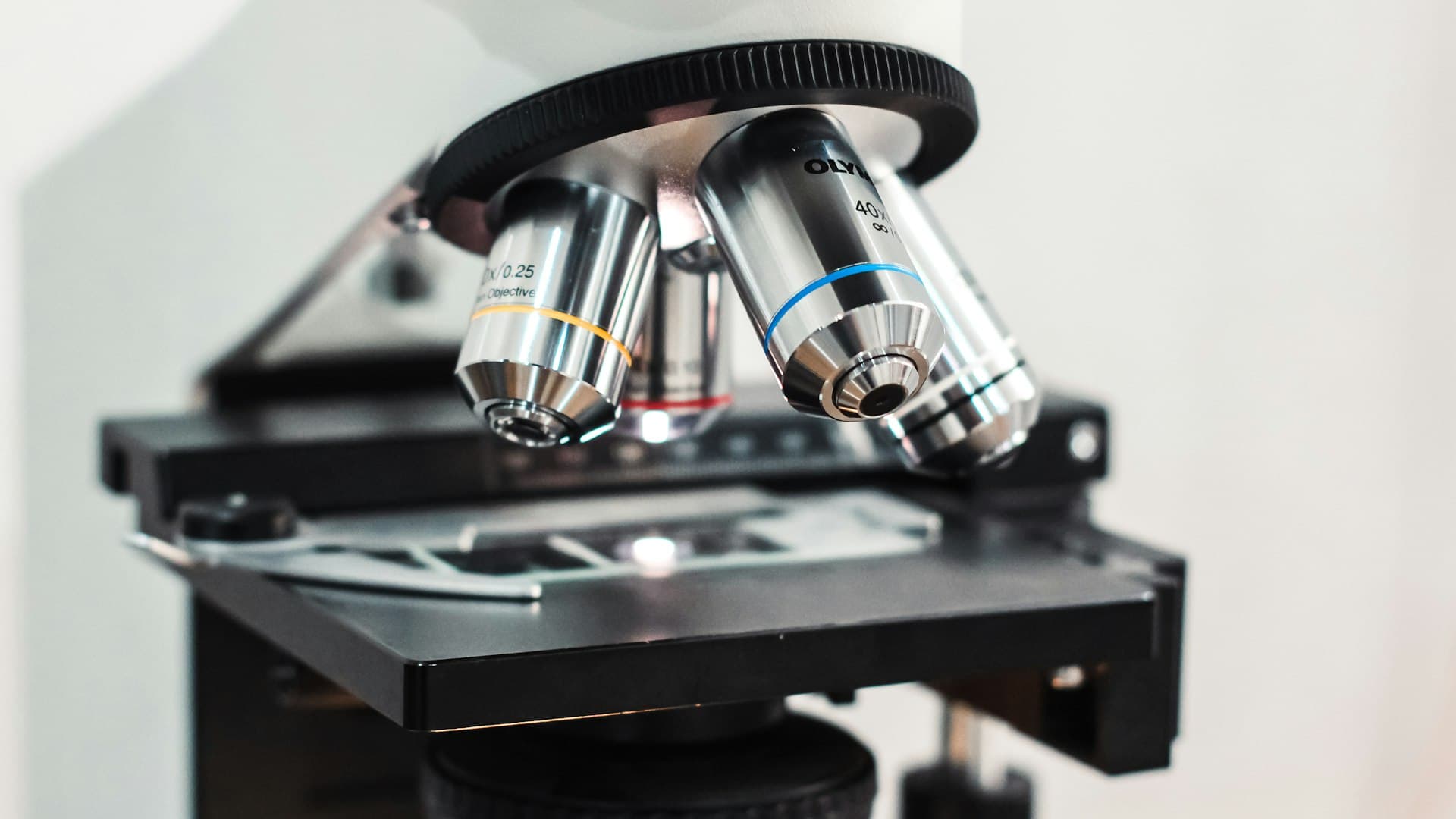
Nanotechnology has attracted more forecasting than any material topic of the last thirty years, and the useful way to think about it in workforce terms is considerably more modest than the forecasts.
The job title that barely exists
Very few organisations advertise for a nanotechnologist. They advertise for a process engineer in a semiconductor fab, a formulation scientist working with nanoparticle dispersions, a materials characterisation specialist, a coatings engineer or a drug delivery scientist.
All of those are nanotechnology jobs and none of them is called that.
Treating nanotechnology as a sector produces a workforce plan with nowhere to put the people. Treating it as a capability inside your existing functions produces one that works.
Which means the practical question for an organisation is not whether to build a nanotechnology capability. It is which of its existing teams need to understand the nanoscale to do their jobs properly.
What the direction covers
The scope: materials at the nanoscale, fabrication, characterisation, nanoelectronics and nanomedicine.
Four areas.
Nanoscale phenomena. Why properties change, covered below.
Fabrication. Top-down approaches such as lithography and etching, and bottom-up approaches including self-assembly and chemical synthesis.
Characterisation. Electron microscopy, scanning probe methods, spectroscopy and scattering. The tools that let you know what you actually made.
Applications. Nanoelectronics, which connects to the semiconductor domain, nanomedicine, which connects to biomaterials and drug delivery, plus coatings, catalysts and composites.
Why small changes behaviour
The physical basis, stated plainly, because it explains both the promise and the problems.
Surface area dominates. As particles get smaller, a larger fraction of their atoms sit at the surface. Since chemistry happens at surfaces, reactivity rises sharply. This is why nanoparticle catalysts work well and also why some nanomaterials are more biologically active than the same substance in bulk.
Quantum effects appear. Below certain sizes, electronic and optical properties become size-dependent. A quantum dot's colour depends on its diameter, which is a property no bulk material has.
Different forces dominate. At this scale, surface forces matter more than gravity, which is why nanoparticles agglomerate and why keeping them dispersed is a central practical problem rather than a detail.
That last point is where a great deal of commercial disappointment comes from. A nanomaterial that performs in a laboratory dispersion frequently agglomerates in a real formulation, and then it behaves like the bulk material you were trying to improve on.
Where this sits in the domain
Nanotechnology is the sixth of eleven directions in Astra Trainer's advanced materials domain, and the one most often scoped as an addition to another direction rather than on its own: with electronic and semiconductor materials, with energy materials for catalysts and battery electrodes, with biomaterials for drug delivery, and with surface engineering for coatings.
Cross-domain, it connects to the semiconductors, electronics and quantum domain, where chip design and semiconductor manufacturing use these tools daily, and to medicine and healthtech. Lessons are five minutes, so laboratory and fab staff add it alongside their existing work. You can see the eleven directions here.
Characterisation is the real bottleneck
The practical constraint in most organisations is not making nanomaterials. It is knowing what you made.
Four reasons.
You cannot see it directly with light. Characterisation means electron microscopy, scanning probe methods or indirect techniques, each with its own preparation requirements and artefacts.
Sample preparation changes the sample. Drying a dispersion for microscopy causes agglomeration, so the image may show something that did not exist in the liquid. Interpreting around that is a skill.
Averages hide distributions. A stated particle size is usually a mean, and performance often depends on the distribution, including the tail of large particles that nobody reports.
Methods disagree. Different sizing techniques measure different things and give different answers for the same sample. Knowing which number means what is a specific competence.
The workforce implication: an organisation buying or making nanomaterials without characterisation capability is accepting supplier claims it cannot check. That is the same problem as the metallurgy certificate of conformity, one scale down.
Safety, which is unresolved and belongs in the training
This section is deliberately uncomfortable, because the honest position is that the science is incomplete.
What is reasonably established: some engineered nanomaterials can behave differently in biological systems than the same substance in bulk form, that inhalation is the main occupational exposure route of concern, and that fibre-shaped nanomaterials have attracted particular scrutiny because of the general concern about durable respirable fibres.
What is not established: a general framework for predicting which nanomaterials are hazardous from their properties, and agreed occupational exposure limits for most of them. Regulatory approaches differ between jurisdictions and continue to develop.
So the responsible practice in industry is control-based rather than limit-based: contain, minimise airborne release, use appropriate ventilation and respiratory protection, and treat powders as the highest-risk form.
A training program that presents nanomaterial safety as a solved problem with known limits is teaching something false. One that teaches the control approach, and is explicit that the hazard picture is still developing, produces people who behave appropriately under uncertainty, which is what the situation actually requires.
The roles, named
Materials characterisation specialists. Electron microscopy and scanning probe work. The broadest demand and a real shortage of people who can interpret rather than operate.
Process engineers in semiconductor fabrication. Nanoscale patterning as daily work.
Formulation scientists working with nanoparticle dispersions in coatings, cosmetics, inks and pharmaceuticals.
Catalysis scientists, connecting to energy and industrial chemistry.
Drug delivery scientists, connecting to biomaterials and pharmaceutical development.
Thin film and coatings engineers.
Cleanroom and nanofabrication facility technicians. Running shared equipment, an underappreciated and consistently needed role.
Occupational hygienists with nanomaterial competence. Small, and needed by anyone handling powders at scale.
Who can be trained into it
Laboratory technicians and microscopists. The shortest route. Already operate the instruments and frequently need the interpretation and artefact awareness.
Chemists. Into synthesis, dispersion and formulation, which is where the practical difficulty lives.
Semiconductor process technicians. Already work at this scale daily and rarely think of it as nanotechnology, which limits where they see themselves being able to go.
Coatings and paint technologists. Into nanoparticle-modified systems.
Pharmaceutical formulation staff. Into nanomedicine and delivery systems.
Occupational hygienists and EHS professionals. Into nanomaterial exposure assessment, which is a genuine gap in most organisations handling these materials.
Exposure control and regulatory status. Engineered nanomaterials are subject to developing and jurisdiction-specific regulation, and agreed occupational exposure limits do not exist for most of them. Handling powders requires containment, ventilation and respiratory protection determined by a competent risk assessment, and specific materials may carry additional controls. Training builds understanding of the hazard picture and of control principles. It does not constitute a risk assessment, exposure limit guidance, or regulatory compliance for any specific material or facility.
What to take from this
Nanotechnology is a capability applied inside other functions, so the workforce question is which of your existing teams need it rather than whether to build a department.
Surface area and quantum effects are why the field exists, and agglomeration is why so much of it disappoints commercially.
Characterisation is the real bottleneck. Without it, you are accepting claims you cannot check.
Scale-up from laboratory to production is where most nanomaterial ventures fail, for the same reason as bioprocessing: the conditions change and the material responds.
And the safety picture is genuinely unsettled, so teach control-based practice and say so, rather than implying limits exist that do not.
Is nanotechnology a career field?
Not as a job title. It is a capability inside semiconductor processing, formulation, characterisation, coatings, catalysis and drug delivery, and that is where the roles are advertised.
Why do nanomaterials behave differently?
Because a large fraction of their atoms sit at the surface, which raises reactivity, and because quantum effects make some properties size-dependent below certain scales.
What limits commercial success most?
Agglomeration and scale-up. A material that performs in a laboratory dispersion frequently clumps in a real formulation and then behaves like the bulk material it was meant to improve on.
Are nanomaterials safe to handle?
The hazard picture is still developing and agreed occupational exposure limits do not exist for most engineered nanomaterials. Responsible practice is control-based: containment, ventilation and respiratory protection, with powders treated as highest risk.
Where does this fit in the domain?
Sixth of eleven directions in Astra Trainer's advanced materials domain, most often scoped alongside electronic materials, energy materials, biomaterials or surface engineering. You can see them here.